A Trustworthy PCB and Electronic Manufacturing Enterprise! Contact Us


In the rapidly shifting landscape of semiconductor manufacturing, the method used to connect an integrated circuit to its environment is as critical as the silicon itself. As microprocessors and memory modules gain more transistors and higher clock speeds, the limitations of traditional "leaded" packages—where metal pins protrude from the sides—have become a major bottleneck. To overcome these constraints, the industry transitioned to the BGA type package, a revolutionary surface-mount technology that utilizes the entire bottom surface of the component for electrical connectivity. Today, this technology is the invisible backbone of high-performance computing, enabling the compact power of everything from professional workstations to the smartphone in your pocket.
Anatomy of a BGA Type Package
At its core, a BGA type package is designed to solve the problem of space. In a standard QFP (Quad Flat Package), the leads are limited to the perimeter of the chip. In contrast, BGA uses an array of microscopic solder balls arranged in a grid across the entire underside.
The internal structure consists of a silicon die attached to a high-density laminate or ceramic substrate. This substrate acts as an intermediary, routing signals from the microscopic pads on the die to the larger solder balls on the bottom. These balls, typically made of tin-silver-copper (SAC) alloys, serve two purposes: they provide the electrical connection to the PCB and act as a mechanical support system that can withstand thermal expansion and contraction.
Technical Superiority of BGA Technology
The adoption of the BGA type package was not merely a choice of convenience but a response to fundamental physical challenges in electronics.
1. Unmatched Electrical Performance
One of the greatest enemies of high-speed digital signals is "lead inductance." Long metal pins act like tiny coils, distorting signals at high frequencies. Because the solder balls in a BGA provide an incredibly short path between the chip and the board, this parasitic inductance is virtually eliminated. This allows for cleaner clock signals and faster data transfer rates, which is why BGA is the standard for DDR5 memory and 5G modems.
2. Efficient Thermal Management
As chips work harder, they generate more heat. In a traditional package, heat must travel through thin metal leads or through the plastic casing to escape. In a BGA type package, the numerous solder balls act as dozens of tiny heat sinks, conducting thermal energy directly into the copper ground planes of the PCB. This efficient heat transfer allows high-performance GPUs and CPUs to maintain peak speeds without overheating or requiring massive external cooling solutions.
3. The Self-Alignment Benefit
During the SMT (Surface Mount Technology) reflow process, the surface tension of the molten solder balls naturally pulls the component into the perfect center of the PCB pads. This "self-alignment" effect significantly reduces manufacturing defects compared to leaded components, where a single bent pin can ruin the entire assembly.
Classification and Material Variations
Manufacturers tailor the bga type package to suit specific environmental and cost requirements. For consumer-grade electronics like laptops and TVs, the PBGA (Plastic BGA) is the most common due to its excellent balance of cost and reliability. However, in the aerospace and defense sectors, where boards face extreme temperature swings, CBGA (Ceramic BGA) is preferred. Ceramic substrates offer superior hermetic sealing and a coefficient of thermal expansion (CTE) that closely matches silicon, preventing cracks in the solder joints over long periods. For ultra-compact mobile devices, FBGA (Fine-pitch BGA) reduces the ball spacing (pitch) to as little as 0.3mm, allowing for even higher component density.

BGA type package
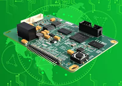
PCB Design Considerations for BGA
Designing a board for a BGA type package is an art form in itself. Because the pins are hidden under the chip, designers must use "fan-out" strategies to route traces from the inner rows of balls to other parts of the board. This often requires high-density interconnect (HDI) technology, utilizing blind and buried vias—tiny holes that only go through specific layers of the board—to manage the complex web of connections. Without these advanced PCB fabrication techniques, it would be impossible to utilize the full potential of high-pin-count BGA devices.
Assembly, Inspection, and Rework
The manufacturing process for a BGA type package requires high-precision equipment. Solder paste must be printed with micron-level accuracy, as even a tiny excess of paste can cause a "bridge" between two adjacent balls under the chip. Since these joints are invisible to the human eye once the chip is mounted, X-ray inspection is the only reliable way to verify quality. X-ray systems allow quality control teams to look through the chip and ensure that every ball has collapsed into a perfect "barrel" shape, indicating a solid metallurgical bond. If a fault is found, specialized rework stations use infrared heat to lift the chip, clean the pads, and replace the component without damaging the surrounding circuitry.
Conclusion
The relentless drive toward smaller and more powerful devices shows no signs of slowing down. As we look toward the future of 6G, artificial intelligence, and edge computing, the role of the bga type package will only become more prominent. By providing the density needed for thousands of connections and the thermal efficiency required for high-speed processing, BGA technology ensures that Moore's Law continues to hold true. For any hardware engineer or product manufacturer, mastering the implementation of the BGA type package is not just an advantage—it is a fundamental requirement for success in the high-stakes world of modern electronics.