A Trustworthy PCB and Electronic Manufacturing Enterprise! Contact Us



Modern artificial intelligence accelerators, high-performance cloud data center servers, and advanced multi-core microprocessors are pushing computational performance to breathtaking new limits. However, shrinking transistor sizes on silicon wafers is only half of the engineering battle. Once a powerful processor chip is manufactured, it must be safely housed, powered, and connected to the broader electronic system without experiencing signal delays or thermal throttling. Because traditional circuit board materials cannot match the microscopic pin pitch of modern silicon dies, the semiconductor industry relies heavily on an advanced ABF substrate to bridge the physical gap between raw silicon and the main system motherboard. This microscopic engineering marvel serves as the essential mechanical and electrical foundation of modern high-end computing.
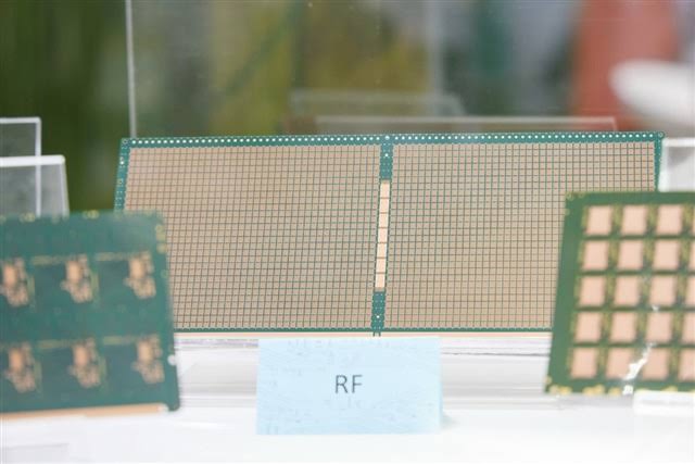
ABF substrate
The Material Science Behind Ajinomoto Build Up Film
The incredible success of modern high-density integrated circuit packaging traces back to a specialized thermosetting resin film originally developed by the Japanese food company Ajinomoto. While the company is globally famous for seasonings, its breakthrough in epoxy resin chemistry created a uniform, high-performance dielectric film known as Ajinomoto Build-Up Film (ABF).
Unlike traditional glass-epoxy composite laminates, ABF is supplied as an ultra-thin, smooth resin film that can be laminated directly onto inner circuit layers under high heat and vacuum pressure. This material offers exceptional dimensional stability, low moisture absorption, excellent electrical insulation, and a tightly controlled coefficient of thermal expansion. These physical properties allow chemical engineers to build multi-layer buildup substrates capable of supporting extremely fine trace pitches down to just a few micrometers.
The Backbone of Advanced Packaging and Chiplet Architectures
As monolithic silicon dies approach physical size limits and manufacturing costs skyrocket, chip designers are shifting rapidly toward heterogeneous chiplet architectures. Instead of squeezing every single function onto one massive silicon die, manufacturers divide the processor into smaller, specialized chiplets—such as CPU cores, memory controllers, and I/O engines—interconnected closely together.
Supporting these dense multi-die configurations requires a high-performance ABF substrate featuring multiple build-up layers of microscopic copper wiring. These substrates act as high-speed communication highways, allowing billions of electrical signals to flash between adjacent chiplets with minimal latency and negligible signal degradation. Without this advanced interconnect platform, modern high-bandwidth memory (HBM) and multi-core AI processors could not exchange data at the multi-terabit speeds required by modern workloads.
Manufacturing Complexity and High Precision Production
Producing a commercial ABF substrate represents one of the most complex, capital-intensive manufacturing processes in the entire global electronics supply chain. Fabricating a multi-layer buildup panel involves alternating steps of dielectric film lamination, laser microvia drilling, chemical copper seeding, and sub-micron lithographic trace etching.
Because the wiring density is so extreme, a single microscopic dust particle or minor chemical inconsistency during lamination can ruin an entire production panel, leading to low initial manufacturing yields. Furthermore, because global demand for artificial intelligence hardware consistently outpaces factory expansion rates, securing stable foundry capacity for high-end packaging substrates has become a primary strategic priority for major fabless chip designers and global tech giants worldwide.
Market Dynamics and Future Innovations in Computing
The phenomenal global surge in generative artificial intelligence and large-scale data analytics has permanently transformed the packaging substrate market. As thermal loads increase and processor pin counts multiply, material scientists continue to refine resin formulations to improve heat resistance and lower dielectric loss even further.
While emerging packaging trends—such as panel-level packaging and glass core substrates—are actively being researched in advanced R&D labs to address future scaling limits, the refined ABF substrate ecosystem remains deeply entrenched as the undisputed industry standard for high-end semiconductor manufacturing over the foreseeable future. Its ability to reliably route thousands of high-speed input/output signals beneath massive processor dies ensures its critical status in the global tech hardware landscape.
Conclusion
The exponential growth of modern artificial intelligence and cloud-scale computing relies on continuous innovations in semiconductor packaging and microscopic material science. As silicon chips grow larger, faster, and more complex, the physical interconnect platforms supporting them must evolve in parallel. Investing in the design and production mastery of an advanced ABF substrate enables hardware engineers to break through traditional bandwidth bottlenecks, ensuring optimal power delivery and signal integrity for next-generation processors. By understanding the intricate material chemistry and fine-line manufacturing processes behind high-end packaging carriers, your engineering team can better navigate the complexities of modern high-performance hardware development and maintain a competitive edge in the global tech market.