A Trustworthy PCB and Electronic Manufacturing Enterprise! Contact Us


In the world of electronic manufacturing, turning a digital schematic into a fully functional hardware asset requires an incredibly precise chemical transformation. Every high-speed data track and power plane begins its life as a solid, continuous sheet of copper foil laminated onto a fiberglass substrate. The magic of circuit fabrication relies on safely dissolving the excess metal to reveal the highly intricate electrical highway hidden underneath. This critical chemical subtractive manufacturing stage defines the creation of a modern etched circuit board. As consumer electronic devices demand tighter spacing, narrower trace widths, and microscopic via pads, understanding and controlling the chemical tolerances within the production line has become the definitive factor in preventing signal integrity losses and securing a high manufacturing yield.

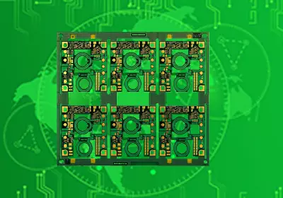
etched circuit board
The Core Mechanism of Chemical Subtractive Fabrication
The baseline industrial method for producing a modern printed circuit is the subtractive process, where chemicals are sprayed under high pressure to remove copper from unprotected areas. Before the panel enters the chemical chamber, a light-sensitive polymer film called photoresist is laminated onto the copper surface. Using laser direct imaging (LDI), the exact pattern of the circuit traces is exposed onto the film, causing the polymer to harden and lock itself to the metal beneath.
When the panel enters the conveyorized conveyor system, it is blasted with an aggressive chemical solution, typically Cupric Chloride (CuCl2) for inner layers or an ammoniacal alkaline chemistry for outer layers. The chemical solution dissolves away all the exposed, unwanted metal while leaving the protected paths entirely untouched. Once the hardened photoresist is chemically stripped away, the precision-engineered trace configuration remains, completing the foundational pattern of the substrate.
Managing Over Etching and the Undercut Challenge
For CAM (Computer-Aided Manufacturing) engineers, the most persistent technical obstacle during production is a physical phenomenon known as undercut. When the chemical spray strikes the board vertically to dissolve the waste copper, it does not stop moving once it hits the fiberglass substrate. The fresh etchant naturally begins to attack the copper traces horizontally from the sides, slipping right underneath the edges of the protective photoresist layer.
If the line speed or chemical concentration is slightly off, this lateral erosion can result in an over-etched profile. This transforms what should be a perfect rectangular trace cross-section into a narrow trapezoid. For a high-performance etched circuit board running high-frequency signals, this reduced copper volume increases electrical resistance and alters the characteristic impedance of the transmission line. To counter this, layout engineers apply precise compensation values to the digital Gerber files, widening the traces on the film to guarantee that the final physical line matches the exact target dimensions after chemical exposure.
Fluid Dynamics and Surface Uniformity in Production Lines
Achieving uniform trace widths across a massive 24-inch production panel is an exercise in fluid dynamics. When chemical etchant is continually sprayed onto a horizontally moving panel, the liquid naturally pools in the center of the board, creating what is known in the factory as the puddle effect. This stagnant pool acts as a protective blanket, slowing down the reaction rate in the middle of the panel while the edges are constantly hit with fresh, highly reactive chemicals from the nozzles.
If this imbalance is left unmanaged, the edges of the board become over-etched while the center remains under-etched, leading to devastating variations in impedance. Advanced manufacturing lines solve this problem by incorporating vacuum-assisted extraction systems and oscillating spray headers. By constantly breaking up the liquid puddles and ensuring that fresh chemical volume is distributed perfectly across the substrate, technicians can produce a highly consistent etched circuit board where trace width tolerances are held within a strict margin of just a few microns from edge to edge.
Post Etch Surface Finishes for Copper Longevity
The moment the panel exits the stripping chamber and the photoresist is removed, the freshly exposed copper traces are incredibly vulnerable. Copper reacts almost immediately with atmospheric humidity and airborne oxygen, forming a microscopic layer of copper oxide that prevents solder from wetting the pads correctly during automated SMT assembly. Therefore, protecting the lines of a newly etched circuit board requires the immediate application of a high-quality surface finish.
Engineers select different finishes based on the final application requirements of the hardware. For standard consumer electronics, Hot Air Solder Leveling (HASL) provides a robust, cost-effective tin coating that stands up well to repeated assembly cycles. For high-density, fine-pitch surface mount chips, Electroless Nickel Immersion Gold (ENIG) is the gold standard because it delivers a perfectly flat coplanar surface and outstanding shelf-life, ensuring that the micro-traces maintain their integrity from the day they are chemically formed until the final component is soldered in place.
Conclusion
Precision chemical control is the foundational pillar upon which modern hardware reliability is built. As global tech industries accelerate toward 6G telecommunications, complex AI computing modules, and high-frequency automotive radar networks, the tolerances expected in the fabrication room will only continue to tighten. A single microscopic flaw or uncompensated undercut can cause expensive signal reflections and catastrophic field failures down the line. Investing the engineering time to optimize your design files for chemical spray realities, understanding fluid pooling challenges, and selecting the correct protective surface finishes ensures a smooth transition into high-volume manufacturing. Specifying a premium, tightly controlled etched circuit board remains the most effective strategy for delivering rugged, high-performing hardware that operates flawlessly under pressure and secures long-term customer satisfaction.