A Trustworthy PCB and Electronic Manufacturing Enterprise! Contact Us


In standard circuit manufacturing, the primary goal of the fabrication line is to cover as much bare metal as possible with a protective layer of solder mask. This insulating barrier keeps the delicate circuit paths safe from oxidation and prevents catastrophic solder bridges during automated assembly. However, as modern electronics push the limits of power density—such as in electric vehicle motor controllers, high-current power supplies, and high-brightness LED modules—standard insulation can trap destructive amounts of thermal energy. To overcome this limitation, hardware engineers often deliberately create windows in the solder resist layer to produce an exposed copper PCB. By strategically leaving specific areas of the copper traces completely bare, designers can radically improve the thermal dissipation, current-carrying capacity, and shielding efficiency of their high-performance hardware systems.

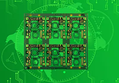
exposed copper PCB
Thermal Management and Heat Dissipation Solutions
The primary motivation behind removing the solder mask to reveal raw copper is thermal management. While standard liquid photoimageable (LPI) inks are excellent electrical insulators, they double as thermal insulators, meaning they trap heat at the semiconductor junction. For a power component like a surface-mount MOSFET, operating temperatures can quickly skyrocket if heat cannot escape into the surrounding environment.
Leaving a wide area of copper bare around the component pad changes the thermal dynamics entirely. Air can now circulate directly over the highly conductive copper surface, carrying away heat much faster than through a layer of polymer ink. Furthermore, an exposed copper PCB allows for direct metal-to-metal contact when mounting external copper or aluminum heat sinks. By eliminating the thermal resistance of the solder mask layer, the heat transfer efficiency is maximized, lowering the component junction temperature and significantly extending the operating lifespan of the entire electronic system.
Maximizing Current Carrying Capacity through Solder Layering
Another brilliant, cost-effective engineering hack made possible by an exposed copper PCB is the ability to drastically boost trace current limits without upgrading to expensive heavy-copper substrates. Typically, if a design requires a trace to carry 30 A of continuous current, an engineer would have to specify a thick 3 oz or 4 oz copper layer, which heavily inflates the fabrication budget and limits the fine-pitch routing capabilities of other signals on the same board.
By opening the solder mask over the power rail, the factory leaves a long channel of bare copper exposed. During the wave soldering or surface-mount reflow process, liquid solder naturally pools and adheres to this exposed line, creating a thick, raised layer of solder directly on top of the copper trace. Since solder is highly conductive, this added metal thickness drastically reduces the overall electrical resistance of the trace, allowing it to handle massive current surges with minimal temperature rise, saving significant manufacturing costs.
Radio Frequency Shielding and Grounding Integrity
In high-frequency telecommunications and aerospace applications, exposed copper areas serve a critical electrical purpose rather than just a thermal one. Radio frequency (RF) signals require an incredibly low-impedance ground return path to prevent signal distortion and electromagnetic interference (EMI). Any insulating barrier between the ground plane and a shielding component can compromise the integrity of the system.
When building a high-frequency exposed copper PCB, engineers design bare copper borders around sensitive circuit blocks like local oscillators or amplifiers. This continuous, uninsulated metallic strip serves as the perfect mechanical and electrical landing pad for surface-mount shielding cans. Soldering the metal cage directly onto the exposed copper ground creates an airtight Faraday cage that successfully blocks external EMI and prevents internal high-frequency noise from escaping into adjacent circuits.
Surface Finishes for Exposed Copper Protection
Leaving copper bare during the board layout process means that the factory must apply a high-quality surface finish to prevent the exposed metal from oxidizing before it can be soldered or integrated into the final assembly. Copper reacts rapidly with atmospheric oxygen, forming a non-conductive oxide layer that ruins solderability.
Engineers generally select Electroless Nickel Immersion Gold (ENIG) for premium applications because the flat gold layer provides excellent oxidation resistance and a perfectly flat surface for component mounting. For cost-sensitive designs, Hot Air Solder Leveling (HASL) provides a robust alternative by pre-coating the exposed zones with a durable tin-lead or lead-free alloy layer. Regardless of the finish choice, specifying precise tolerances for the solder mask clearance ensures that the boundaries of the exposed zones remain sharp and clear, preventing accidental shorts with nearby fine-pitch routing lines.
Conclusion
Striking a perfect balance between robust insulation and high-performance conductivity is the ultimate goal of advanced electronic packaging. While standard solder mask coatings remain perfect for low-power digital signals, the unique demands of heavy power distribution, extreme thermal loads, and sensitive radio frequency systems necessitate a more strategic approach. Integrating a professionally configured exposed copper PCB layout into your hardware development cycle gives you the freedom to handle immense currents, eliminate expensive cooling components, and secure clean, noise-free signal transmission paths. By understanding when and where to drop the protective mask, hardware developers can deliver highly optimized, commercial-grade electronics that excel in the field. Ultimately, spending the extra engineering time to plan your exposed copper areas is an investment in the long-term reliability and manufacturing efficiency of your product line.