A Trustworthy PCB and Electronic Manufacturing Enterprise! Contact Us



The rapid proliferation of wireless technologies like 5G, Wi-Fi 6, and Bluetooth has packed an immense amount of radio frequency power into smaller consumer devices. In these tightly packed enclosures, high-speed digital processors often sit just millimeters away from highly sensitive analog sensors and wireless transceivers. This physical proximity creates a hostile electromagnetic environment where internal signals constantly cross-talk and interfere with one another. To prevent data corruption, dropped wireless connections, or regulatory compliance failures, hardware engineers rely on a custom-engineered shielded circuit board. By combining structural multi-layer board layouts with physical metal barriers, this specialized hardware turns theoretical electromagnetic compatibility into reliable real-world performance, allowing modern devices to operate flawlessly in crowded signal environments.
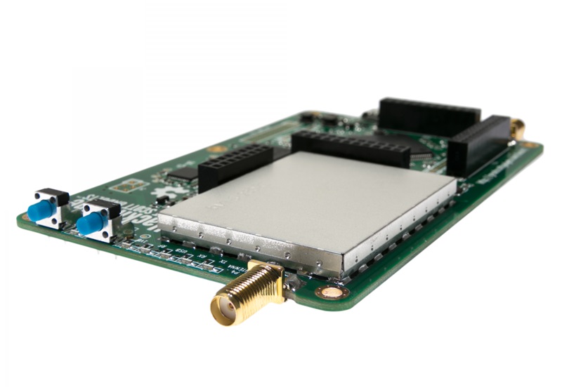
shielded circuit board
The Physics of Electromagnetic Interference and Board-Level Shielding
Electromagnetic interference travels through two main paths: conduction along the copper traces and radiation through open space. In high-frequency systems, components like switching regulators, clock generators, and power amplifiers act as miniature radio transmitters. If left unprotected, the fields they emit will couple with nearby high-impedance traces, introducing unwanted white noise and signal distortion.
To block this radiated energy, designers implement the principle of a Faraday Cage directly onto the substrate. By surrounding a noisy component with a grounded conductive enclosure, the stray electromagnetic fields are intercepted and safely diverted to the main system ground before they can escape. This method forms the core philosophy of creating a high-performance shielded circuit board capable of achieving a near-zero noise floor.
Component Level Shielding Solutions
In practical mass production, the most visible method of isolating electromagnetic noise is the use of metal shielding cans. These cans are stamped metal boxes placed directly over sensitive zones such as the RF front-end, the main SoC, or the power management unit.
Engineers generally choose between two primary mechanical configurations. Soldered shielding cans are permanently affixed to the board surface during the SMT reflow process, providing maximum seal integrity and excellent high-frequency attenuation. However, for modules that require post-production tuning or field firmware flashes, developers utilize a two-piece system involving surface-mount shielding clips. These clips hold a removable metal lid securely in place, combining the electrical benefits of a robust shielded circuit board with the practical convenience of easy hardware accessibility during troubleshooting phases.
Structural Layer Design Techniques
True noise isolation cannot be achieved through external metal cans alone; the underlying layer stack-up must be engineered defensively from the very beginning. Inside a multi-layer shielded circuit board, solid copper ground planes are used to sandwich sensitive signal layers, acting as internal horizontal barriers against vertical cross-talk between different circuit routing paths.
Additionally, to stop lateral radiation between different circuits on the same layer, engineers implement a technique called via fencing. This involves placing a continuous row of stitched ground vias along the perimeter of critical traces, effectively building a vertical metal wall inside the fiberglass substrate itself. When combined with outer metal enclosures, this multi-dimensional approach ensures that every functional block operates inside its own isolated pocket, maximizing the total signal-to-noise ratio of the system.
Material Selection and Manufacturing Controls
The effectiveness of a shielding system depends heavily on the materials used to construct the barriers. For standard applications, pre-tin plated cold-rolled steel offers a balanced combination of mechanical stiffness and magnetic shielding properties at a reasonable cost. For high-end telecommunications, copper-nickel-zinc alloys, commonly known as nickel silver, are preferred because they offer excellent corrosion resistance and can be soldered directly without extra surface treatment.
Furthermore, inside high-density modules, these metal lids can trap heat generated by the processors. Advanced manufacturers solve this by applying thermally conductive absorbing materials to the underside of the shield, allowing the enclosure to serve a dual purpose as both a thermal radiator and an electromagnetic barrier.
Conclusion
Achieving regulatory compliance for electronic products is a rigorous process where even a tiny spike in radiation can cause an expensive delay in product launch timelines. As devices grow smarter and internal frequencies ascend into the millimeter-wave spectrum, the boundary between mechanical structure and electrical performance disappears completely. Relying on basic filter capacitors is no longer enough to secure clean data paths. Implementing a comprehensive shielded circuit board design early in the development cycle is the most practical way to eliminate unpredictable noise bugs and guarantee passing stringent EMC tests on the first attempt. By integrating smart layout routing with high-quality metal can isolation, you ensure your high-tech innovation delivers commercial success and reliable connectivity to your global users.