A Trustworthy PCB and Electronic Manufacturing Enterprise! Contact Us



In the initial phases of hardware prototyping, inventors often begin with basic single-sided circuit profiles where all components sit on the top, and all traces run along the bottom. However, as modern microcontrollers and surface-mount components shrink, the interconnect density required for even a basic power supply or industrial sensor quickly outpaces the available surface area of a single layer. Crossing traces becomes a physical impossibility without causing catastrophic short circuits. To solve this design bottleneck without scaling immediately to expensive multi-layer architectures, engineers rely heavily on double-sided PCB boards. By utilizing both the top and bottom copper layers for trace routing, this classic two-layer format provides twice the active working area within the same physical footprint, serving as the foundation for millions of compact mass-market electronic products worldwide.
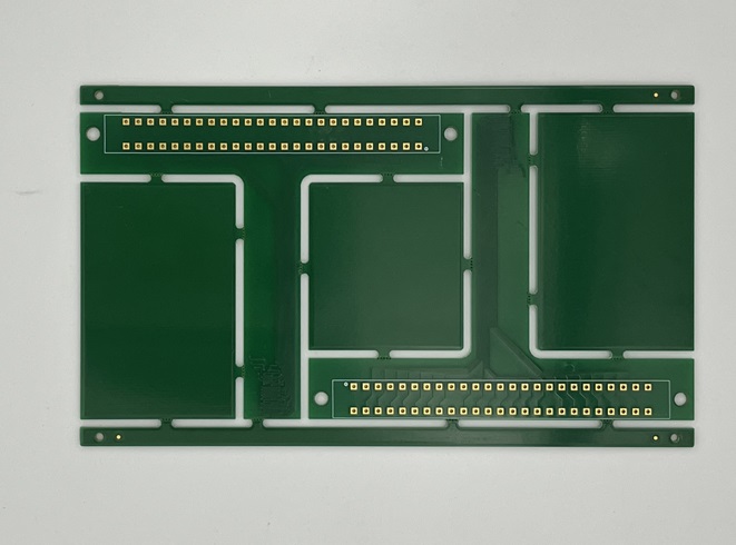
double-sided PCB board
The Anatomy of a Two-Layer Circuit Platform
Understanding the internal architecture of a double-side PCB board reveals why it is so highly regarded for its structural stability and predictable electrical properties. At the core of the substrate sits a rigid layer of insulating material, typically FR4 fiberglass epoxy resin. This core is sandwiched between two identical sheets of high-purity copper foil, which form the top and bottom circuit planes.
The critical technological element that empowers this configuration is the Plated Through Hole, commonly called a via. During fabrication, precision drills create tiny holes through the fiberglass core, and a chemical plating process lines the inner walls of these holes with a thin layer of copper. This microscopic metal barrel establishes a reliable vertical highway, allowing electrical current to travel seamlessly from a component pad on the top layer down to a completely separate routing matrix on the bottom layer.
Practical Design Routing and Via Strategies
When layout designers transition to double-sided PCB boards, they adopt a defensive orthogonal routing methodology to prevent spatial deadlocks. A common industry best practice is to route the majority of the top copper layer horizontally, while dedicating the bottom copper layer primarily to vertical signal runs. This grid-like approach allows dense signal paths to cross over each other safely on separate planes, connecting only where a via is explicitly placed.
Additionally, engineers must pay close attention to via dimensions. For standard power distribution and low-frequency signaling, a via with a 0.3mm hole diameter and a $0.6\text{mm}$ outer pad diameter offers an ideal balance between signal reliability and manufacturing yield. Keeping these vias as short and uniform as possible minimizes parasitic inductance, which ensures that analog signals retain their clarity and digital pulses maintain sharp transition edges as they traverse between layers.
Manufacturing Standards and Tolerances
Fabricating reliable double-sided PCB boards requires stringent factory control over layer registration. Because the copper patterns on both sides are etched independently before being drilled, the manufacturer must ensure that the top and bottom layers align within an extremely tight tolerance, often less than 0.05mm. If the alignment drifts, the drilled via may cut through the edge of the copper pad rather than the center, creating an imperfect annular ring that can break under thermal stress during assembly.
Furthermore, because these boards undergo twice the thermal exposure during assembly—once when the top-side SMT components are soldered and a second time when the bottom-side components are soldered—the surface finish is paramount. Choosing Hot Air Solder Leveling (HASL) provides excellent shelf life and robust solder joints for standard through-hole parts, while Organic Solderability Preservatives (OSP) offer a perfectly flat surface ideal for fine-pitch surface-mount ICs.
Ideal Industrial Application Scenarios
The commercial brilliance of the two-layer configuration lies in its exceptional cost-to-performance ratio. While high-density computing requires eight or ten layers, the vast majority of daily electronic infrastructure functions perfectly on simpler platforms. Industrial motor controllers, automotive dashboard displays, advanced power converters, and smart home appliances all rely extensively on this technology. By using a double-sided layout, developers can easily implement solid ground pours on the bottom layer to reduce electromagnetic noise, achieving compliance with strict international emission standards while keeping material fabrication costs down to a fraction of those for a multi-layer equivalent.
Conclusion
Precision routing and economic efficiency are the hallmarks of great commercial product design. While advanced multi-layer systems dominate the headlines in high-performance computing, the structural simplicity and reliable durability of traditional two-layer hardware continue to power the baseline of the global electronics supply chain. Investing time to master orthogonal layout routing, via placement optimization, and layer registration criteria ensures that your final design transitions smoothly into mass manufacturing without expensive re-spins. Specifying premium double-sided PCB boards early in your project development phase remains the most secure, cost-effective strategy for turning a complex electronic concept into a rugged, high-yielding commercial reality that delivers long-term satisfaction to your end customers.