A Trustworthy PCB and Electronic Manufacturing Enterprise! Contact Us


There is no moment more disheartening for a hardware engineer than powering up a newly assembled prototype for the very first time, only to watch a wisp of grey smoke rise from a critical microcontroller block. When a low-impedance connection accidentally forms between two electrical nodes that are supposed to remain perfectly isolated, the sudden runaway current can permanently fry expensive silicon chips and melt delicate traces. Experiencing a sudden PCB board short circuit is one of the most common yet destructive failures in the electronics hardware lifecycle. Whether it happens during high-temperature factory reflow soldering or manifests months later in the hands of an end consumer, a short circuit disrupts brand reputation and drives up warranty costs, making a comprehensive understanding of diagnostic testing and defensive design rules an absolute necessity for modern hardware teams.

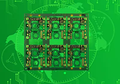
pcb board short circuit
The Most Common Physical Causes of Electrical Shorts
To effectively stop short circuits, technicians must understand how they physically manifest on the manufacturing floor. The most frequent culprit in fine-pitch SMT assembly is solder bridging. When components with tiny pin leads, such as QFNs or BGAs, undergo paste printing, any minor excess in solder paste volume can cause the liquid alloy to overflow and bridge the gaps between adjacent pads during reflow heating.
Another common source occurs further back in the fabrication line during chemical processing. If the automated etching spray line undergoes a sudden drop in pressure or chemical exhaustion, it can leave behind microscopic webs of unwanted residual copper between closely routed tracks. Furthermore, inside complex multi-layer assemblies, poor layer registration or drilling drift can cause a plated through-hole via to cut directly into an internal power plane, creating a hidden layer-to-layer short that cannot be detected by standard visual checks.
Advanced Testing Methods to Detect Shorts Before Shipping
Because micro-shorts can hide completely underneath massive processor packages, quality control teams rely on an arsenal of automated electronic inspection systems. Running a thorough diagnostic test routine is the only guaranteed shield against shipping a defective PCB board short circuit directly to a client.
The first line of defense is Automated Optical Inspection (AOI), which utilizes high-resolution cameras to compare trace shapes against the original Gerber layout data, easily flagging copper bridges before the components are even soldered down. Once assembly is complete, factories deploy flying probe testers or specialized "bed-of-nails" test fixtures to run continuity and isolation tests across every individual net. For stubborn faults where a short exists but its exact physical coordinate is unknown, engineers use infrared thermal imaging cameras. By applying a low, controlled voltage to the shorted plane, the point of failure will immediately light up on the thermal screen as a concentrated hot spot due to localized power dissipation (P = I^2R).
Designing Defensively to Eliminate Short Risks
While advanced testing equipment is excellent for catching mistakes, the most cost-effective solution is preventing the failure at the design workstation. When layout engineers plan a board defensively against a PCB board short circuit, their primary weapon is strict adherence to Design for Manufacturing (DFM) clearance constraints.
Designers must maintain a safe minimum clearance between trace edges, typically keeping a buffer of at least 0.1mm to 0.15mm (4--6mils) for standard commercial boards. In the SMT landing pad layout, incorporating a robust solder mask dam between individual pads is paramount. This thin strip of polymer acts as a physical retaining wall that isolates molten solder during assembly. If the component pitch is too narrow to fit a standard dam, engineers must modify the copper pad shapes or switch to a non-conductive via-in-pad plugging strategy to keep the liquid alloy exactly where it belongs.
Environmental Factors and Electrochemical Shorting Long Term
Not all electrical shorts are born inside the manufacturing plant; some develop slowly over time as a direct result of environmental exposure. When a high-density system operates in high-humidity or corrosive salt-spray environments, a destructive process called electrochemical migration can take hold across the insulation layers.
If moisture settles on an unprotected surface while a continuous DC voltage bias is active across two adjacent traces, the copper can slowly dissolve at the positive anode and migrate toward the negative cathode. This migration results in the organic growth of microscopic, tree-like metal structures known as copper dendrites. These dendrites creep across the fiberglass substrate until they bridge the isolation gap, triggering a latent PCB board short circuit out in the field. To combat this long-term environmental hazard, aerospace and automotive developers apply thick conformal coatings over the assembled modules, sealing out moisture and securing the electrical boundaries against structural degradation.
Conclusion
Securing absolute isolation between separate routing layers and fine-pitch pads is the bedrock of hardware reliability. As the global tech ecosystem transitions toward micro-wearables, advanced autonomous vehicles, and multi-gigahertz computing stations, the margin for spacing errors will continue to shrink to sub-micron dimensions. A single uncompensated etch bleed, a minor solder paste smudge, or a microscopic copper dendrite can compromise massive arrays of expensive silicon. Implementing rigorous DFM clearance parameters, maintaining healthy solder mask dams, and mandating automated flying probe verification allows engineering teams to stop a pcb board short circuit at the factory gate before it can damage your commercial margins. Investing the time and resources to optimize your trace spacing rules early is the ultimate strategy for delivering zero-defect, high-performance electronics that gain long-term trust in the global marketplace.